- Home»
- An Introduction to Our Technology»
- High Density Fine Circuir Pattern Technology
Features
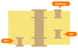
- Satosen offers multi-layer high-density/IVH/BVH/build-up printed circuit boards that allow for a high degree of freedom when it comes to design.


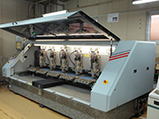
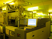
- With its ultra-high speed small caliber rotary drilling machinery, high-density circuit formation (L/S = 30μ/40μ) using LDIs (Laser Direct Imaging Devices), x-ray origin drilling equipment and high-density, multi-layered print circuit boards of stable quality, Satosen is able to provide improved hole position quality.

- With flat plugs (Pad on Via), components assembly over through hole becomes possible.
- Through the use of landless through holes, narrow-pitch patterns are supported.
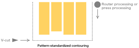
- With CCD, accuracy improvements are made possible for presses, routers and V-cuts(±75) so as to match pattern positions.

- Super-fine printing technology
As its traceability management of manufactured goods , Satosen carry out traditional silk and other forms of printing for large-size printed circuit boards.
However, small-size printed circuit boards really struggled with the printing of individual characters.
Satosen is well-equipped for super-fine printing jobs and has effective methods for dealing with the traceability of individual printed circuit boards.


